Build log

Building in the open.

A running record of PrometheusPCB for the people following along: investors, accelerators, and anyone who wants to see where this goes. Milestones, decisions, and dead ends on the way to a desktop ceramic fab, newest first. I'd rather show the work than polish a highlight reel.

16 entries · last updated Aug 4, 2026

Video from the RF lab talk

In the Jul 27 entry we promised video from our talk with Prof. Changzhi Li's RF lab group at Texas Tech. Here it is, the whole conversation.

Fair warning, it's long. I thought about cutting it down and decided not to, because a video of only the encouraging parts is exactly the highlight reel this log said it would never be. So the recording is posted as it happened. The affirmation is in there, that a bench-speed ceramic fab is something the RF side actually wants. So is the pushback, along with a list of hard requirements. Anyone following this project is welcome to listen and judge both for themselves.

If you listen and hear a hole they missed, or one I answered badly, tell me. Criticism still helps me more than praise does.

The full conversation with Prof. Changzhi Li's RF lab group, unedited. Long on purpose.
Watch on YouTube →

Hyrel invited us out to test our paste on their machines

An update on the Hyrel 3D talks from the Jul 30 entry. I sent them a long list of integration questions about their syringe dispensing heads: line geometry, deposit heights, registration, mounting a head on our own motion platform. The answers came back fast, and they were honest ones. Their CTO replied personally and didn't try to sell me anything. He told me the finest line geometry I asked about is possible but not reliable on a paste extruder, and spelled out what it would take in substrate flatness and bubble-free material to even have a shot.

Then the offer: if I come meet them at their headquarters in Norcross, Georgia, and bring our silver paste and our substrate, they'll run test prints with our material on their machines, with their team, for us. That's a chance to test the riskiest assumption in this machine before we've bought anything, on hardware run by the people who built it.

I plan to take them up on it. The timing works, since the custom Dycotec silver is due off manufacture about now. And I won't show up to wing it. I'll bring a test matrix: sweeps of nozzle size, standoff, and speed, printing combs of straight lines and measuring continuity and width on our actual substrate. Whatever numbers come back will pick the dispensing head the machine gets designed around, and they'll go in this log either way.

That makes twice in a week that blunt technical skepticism came with an offer to help test the thing. A vendor who answers "will this work?" with "come measure it with us" is one I want to work with.

A useful no from pulsed power, Hyrel talks, and the materials seat

We sat down with Prof. Michael Giesselmann, former director of Texas Tech's Center for Pulsed Power and Power Electronics, to ask whether our boards fit pulsed power. He found the idea interesting, and his answer was a useful no. Most of the boards his field runs don't need what our machine brings: passives printed into the layers, dense multilayer routing, and a ceramic body built for heat, high frequency, and hermetic sealing. Pulsed power lives on large discrete components and physical spacing, so miniaturized embedded parts solve a problem they don't have. His caveat cut the other way, though: bring those strengths to aerospace, satellite RF, defense radar, or high-temperature electronics, and the need is real.

Then he offered something better than agreement: he wants to test the machine with his research team once it runs. That's the first outside group asking to put hands on it, and it excited us more than a polite yes would have. It's also the second expert in a row to tell us some version of "not my niche, but aerospace and RF would want this." When skeptics keep pointing at the same sectors, we take it as a signal about where this belongs, not a rejection.

On the hardware side, we got in contact with Hyrel 3D, which builds modular research printers around swappable print heads, and we're negotiating price on one of their SDS syringe dispensing heads. They're made for exactly our kind of work: viscous pastes and gels under controlled volumetric dispensing, with a long trail of research labs publishing on them. If the price works, it runs next to the Allstruder in the silver tests and gives us a second dispensing datapoint.

Last, the seat we've been trying to fill since the very first entry in this log. We've found a materials scientist we want as a co-founder. We're in the final conversations now and updating our applications to include her. Details here when it's official. (Update, Aug 3: those conversations ended without a signing. The seat is open again: deep ceramic materials, same as ever.)

Julian Stoller has left, and PrometheusPCB continues solo

Julian Stoller has left PrometheusPCB. We started building together in June and made it official on Jul 1; four weeks later he's moving on, and I'm continuing as sole founder. The deposition and process scope he owned comes back to me. I'm grateful for the work he put in, and the entries he shaped stay in this log exactly as they were written.

Nothing about the thesis or the schedule moves. The Dycotec silver is still in manufacture, the micro-manipulator is still on the bench, and the next target is still a functional part out of the first hand-run prototype.

I'm posting this because a build log that only records the good weeks isn't a build log. The co-founder seat is open again, and it's the same seat as the very first entry: deep ceramic materials, meaning processing, paste rheology, and constrained sintering.

Applied to Y Combinator

We submitted our application to Y Combinator today, for the Fall 2026 batch. Most of what we had to show is already in this log: the supplier, the silver in manufacture, the motion platform, the first fired parts, and the criticism we got along with our answers to it.

One thing we planned for this application didn't happen. The functional Benchy we targeted for July 26 isn't done, because partway through the week we chose to put that time into the MVP machine itself rather than a hand-built demo. The Benchy stays on the list. The order changed.

We also had our talk with Prof. Changzhi Li and three of his research students, and it was a fantastic conversation. It backed up that what we're building is needed, and it gave us concrete requirements from the RF side that our machine can be built to meet. A video with his student is coming soon and we'll post it here.

Whatever YC decides, we keep building.

Dispensing picked: Allstruder now, Techcon TS5000DMP when the data earns it

The silver needs a path out of the syringe, and we've settled how. For the hand-run proofs we're staying open source: the Allstruder, a modular syringe extruder published this January by Thomas Hinton, Daniel Shiwarski, and colleagues under CC BY 4.0. It mounts to nine printer platforms, takes syringes from 0.1 to 100 mL, and builds from printed parts plus off-the-shelf hardware, which is the flexibility hand-run process development needs. Same reasoning as the motion platform: the dispenser isn't our defensible problem, and this one is already solved well enough to build on.

The upgrade path has a name too. The Techcon TS5000DMP is a disposable-material-path rotary auger valve from the industrial dispensing world. An auger valve meters shear-thinning pastes with much finer start/stop control than a syringe plunger, and the disposable fluid path matters when the fluid is silver: nothing to clean out between runs, nothing wasted in a valve body. It's a purchase the process has to earn with data first, not a day-one buy.

With the Dycotec silver in manufacture, this is the hardware it flows through when it lands, and we're genuinely excited to see what the ink does through each: bead width against our 300–400 µm nozzles, start/stop crispness, how much thinner it takes. Those numbers pick the head the machine gets designed around. The turntable below is the Allstruder itself, so the plan has a face.

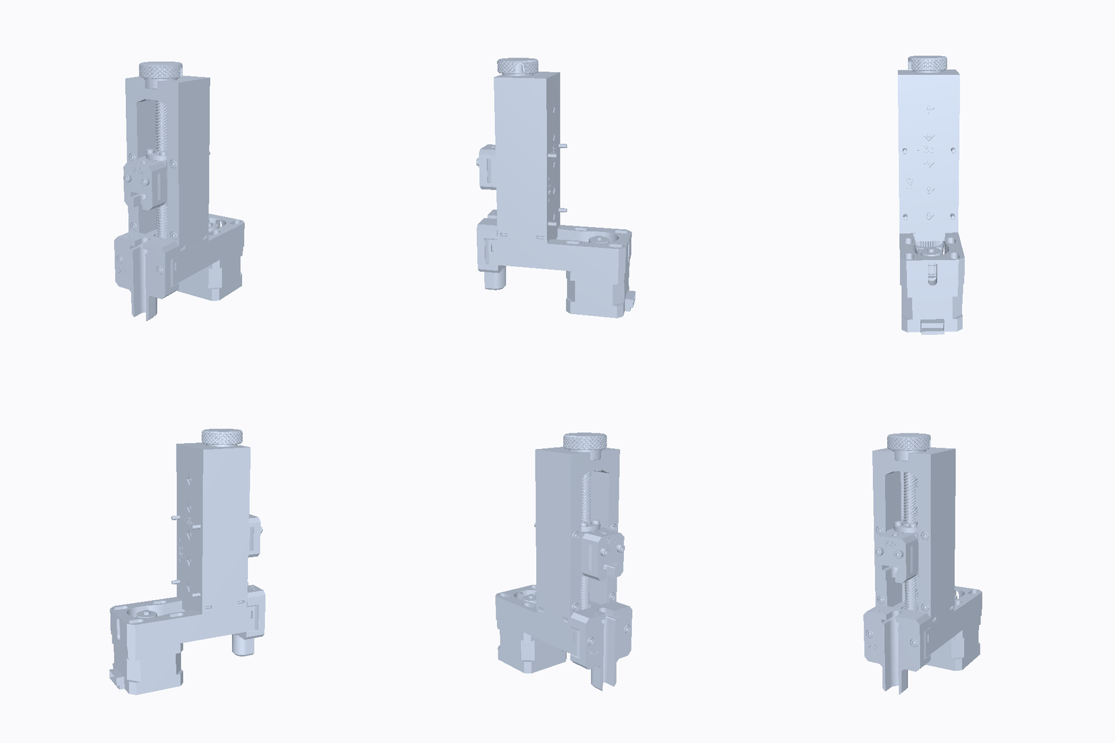
Rotating CAD turntable of the AllStruder syringe-pump extruder: a vertical lead screw and guided plunger carriage above a syringe mount, a knurled adjustment knob on top, and a printable structural body with a mounting base.
The Allstruder in CAD, a lead-screw syringe pump: the screw walks the plunger carriage down the barrel, pushing paste out the nozzle at a rate the motion controller sets, in a body that's mostly printable parts plus off-the-shelf hardware. Design by Hinton, Patten, Crosby, and Shiwarski (CC BY 4.0). This is the design, not our built unit. Build photos when it's assembled and dispensing on the bench.
Allstruder CAD on Zenodo →Techcon TS5000DMP data sheet →

"Elegant on paper, not practical": first expert pushback

The pushback came from someone worth listening to: Tai Phan, Principal Engineer for Electronic Systems at Stalker Radar, with three decades of hardware behind him and, full disclosure, someone Aaron knows from his lab days there. His verdict on PrometheusPCB: elegant on paper, not practical. Industry already has embedded-passive PCB and rarely uses it, because buried parts can't be reworked when a revision swaps one resistor value. The bare board isn't even the expensive part, he added; the components on top are, and you can't recover them by swapping parts from a v1 board onto a v2. And designers won't fly blind on the tolerance, voltage, and wattage of a printed part.

Some of that we accept, some we don't. He's right about production, and we won't pitch this as a way to sustain shipped hardware. We disagree about the loop: when a respin is an afternoon instead of a fab cycle, changing a buried value is a reprint, and a value still being tuned can stay a placed IPC-7351 footprint until it settles. The component-cost point partly lands: printing the passives shrinks what a dead revision wastes, but placed silicon is still lost with the board it's soldered to. That's a real price of iterating, whoever makes the board. On tolerance there's nothing to argue, only to measure: coupons, probe pads, published derating numbers.

What it changed: we didn't file the criticism away. We reached out to Prof. Changzhi Li at Texas Tech ECE, whose field is RF and microwave sensing, and already have a meeting set with him and his research students to put the same objections on the table and see what else breaks.

This log will never be a highlight reel. If you read this and see a hole he missed, tell us. Criticism is worth more to us right now than praise, and we're more motivated with it than we were without it.

Fine-motion platform built, and a first honest look at fired glass

For the MVP we're leaning on open source wherever someone has already solved a problem better than we would. The clearest example is the motion system.

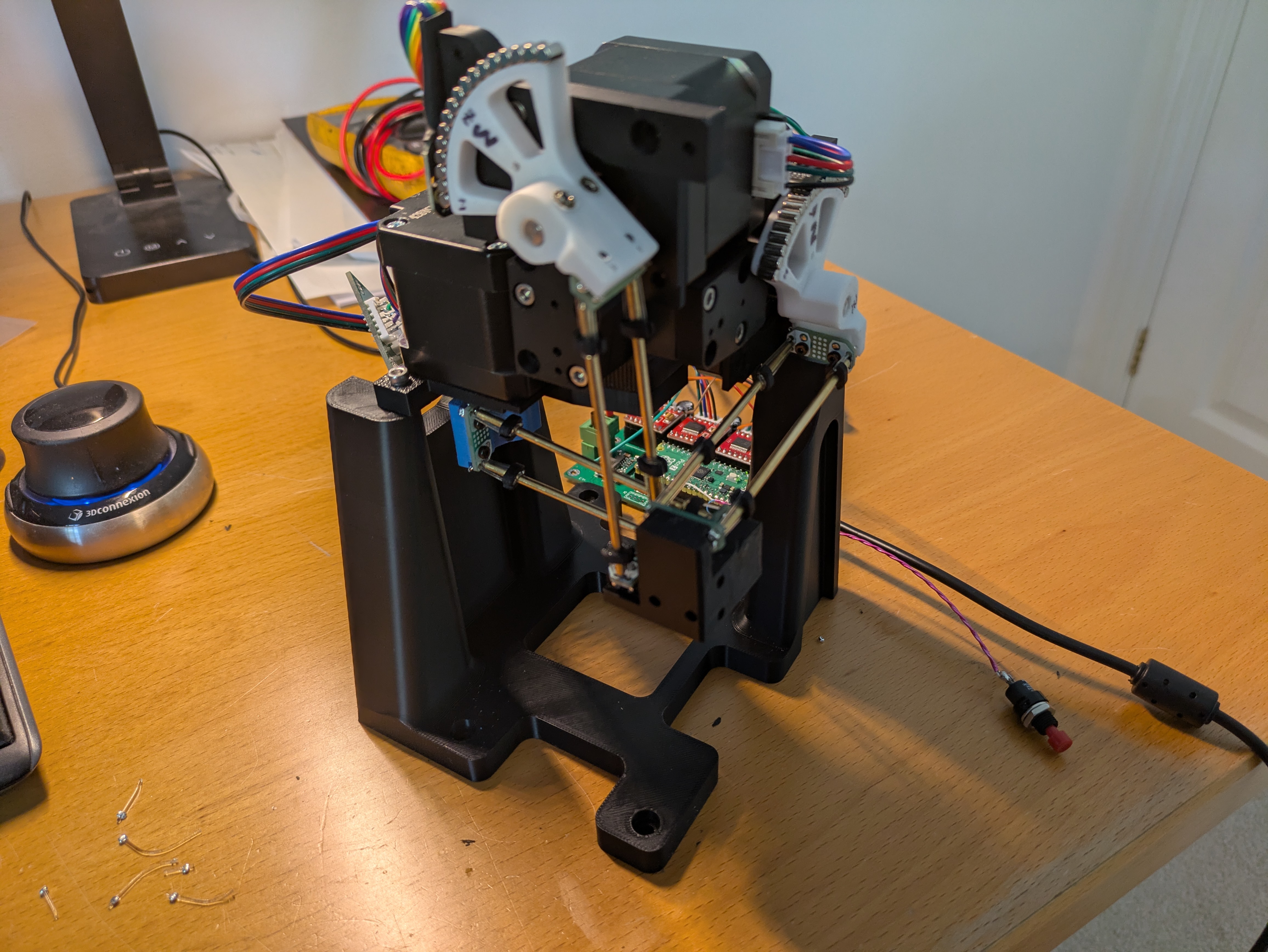
We didn't just pick a stage, we built one. Our fine-positioning platform is 0x23's Open Micro-Manipulator, an open-source parallel-kinematic XYZ design, and the unit in the photo below is our own build: off-the-shelf NEMA-17 steppers, magnetic encoder feedback, a Raspberry Pi microcontroller board, commodity driver modules, a carrier PCB that needs no SMD assembly, and structural parts we printed ourselves.

Building a precision stage from scratch could consume a year. That is not our year of work. The hard problem behind PrometheusPCB is the ceramic and conductor process, not reinventing a gantry. It also isn't a bet on an abandoned repo, and it isn't a bet on paper: the project has ~1.7k stars, 240 forks, an active community, and hardware now at v4.0 with the earlier ball-joint and homing problems already found and fixed by someone other than us, and we've since proven the build is reproducible by doing it ourselves.

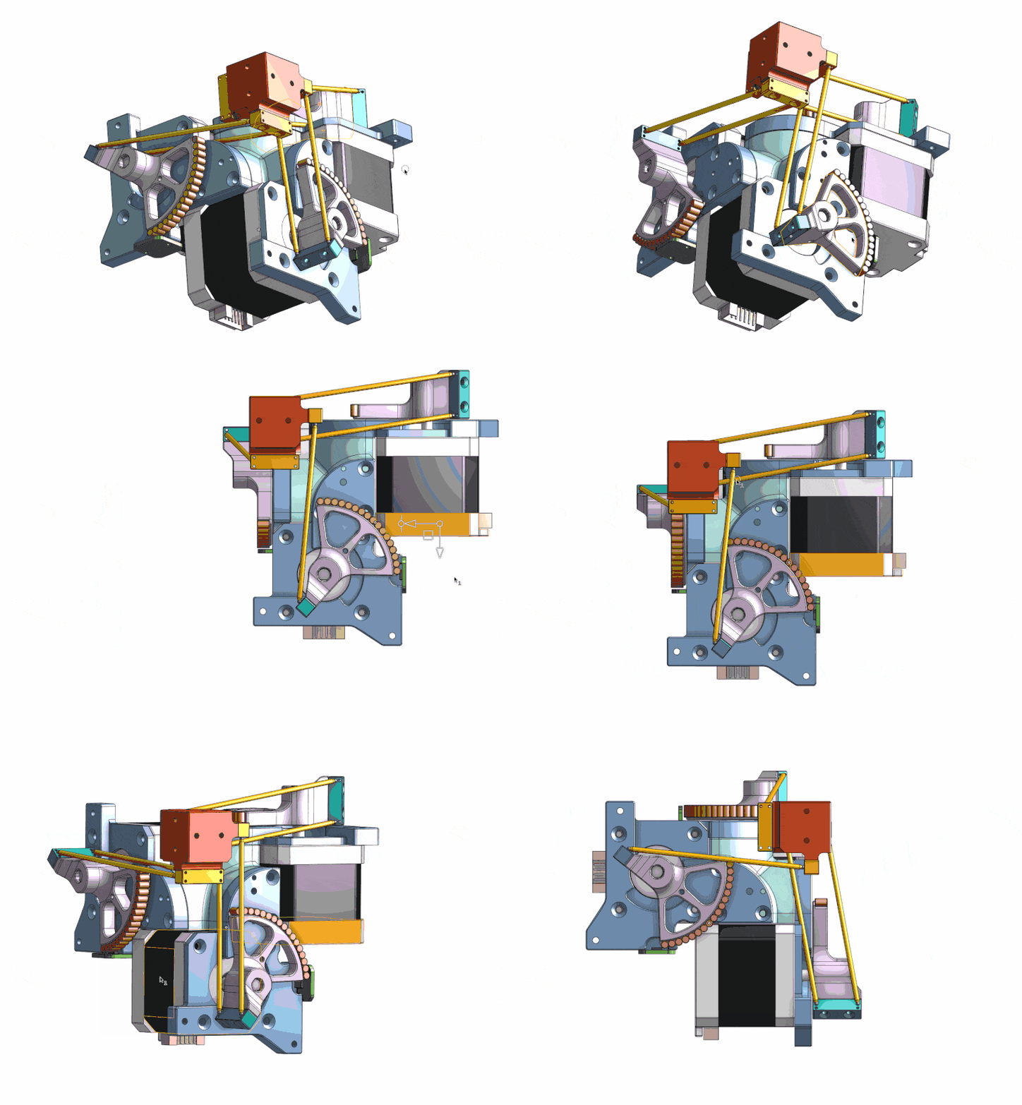
The complete motion architecture is not settled. The manipulator provides fine positioning, but its working area is much smaller than the 200 × 200 mm build area in our concept specification. We see three options: move the platen underneath it with a coarse XY stage, reduce the build area, or modify the manipulator geometry. We're evaluating the usable workspace in CAD, including where the linkages begin to collide; on a parallel mechanism it's self-collision, not motor travel, that sets the real limit. Having the hardware on the bench means we can check those limits against the real thing rather than trusting the model.

Inside that working area the platform gives us considerably more positioning resolution than our process currently needs: commanded steps down to ~50 nm, from magnetic gearing that interpolates low-cost rotary encoders about 30× under a 30 kHz closed loop, against nozzles measured in hundreds of microns. That headroom matters because traces, vias and later dielectric layers must repeatedly land on the same locations. The project correctly distinguishes resolution from accuracy, so our process will rely on part-based fiducials and repeatable local registration rather than assuming perfect global coordinates. If a coarse stage is added, each new working region will be registered back to the part.

The platform also fits our control architecture. It accepts G-code over USB, provides a Python interface, and supports motion-synchronized PWM tool outputs, so dispensing can be timed inside the motion planner rather than controlled independently by the host computer.

On licensing: it's MIT, extended unusually to reach the hardware design and concept as well as the software. Since we've built the design rather than merely referenced it, that attribution is a live obligation and it travels with our documentation. Worth being precise about the limit, since MIT is easy to over-read: it's a copyright grant, not a patent license. Either way we're not trying to build intellectual property around the XYZ stage. Our defensible work is the co-firing process, the material system, and the integrated manufacturing workflow.

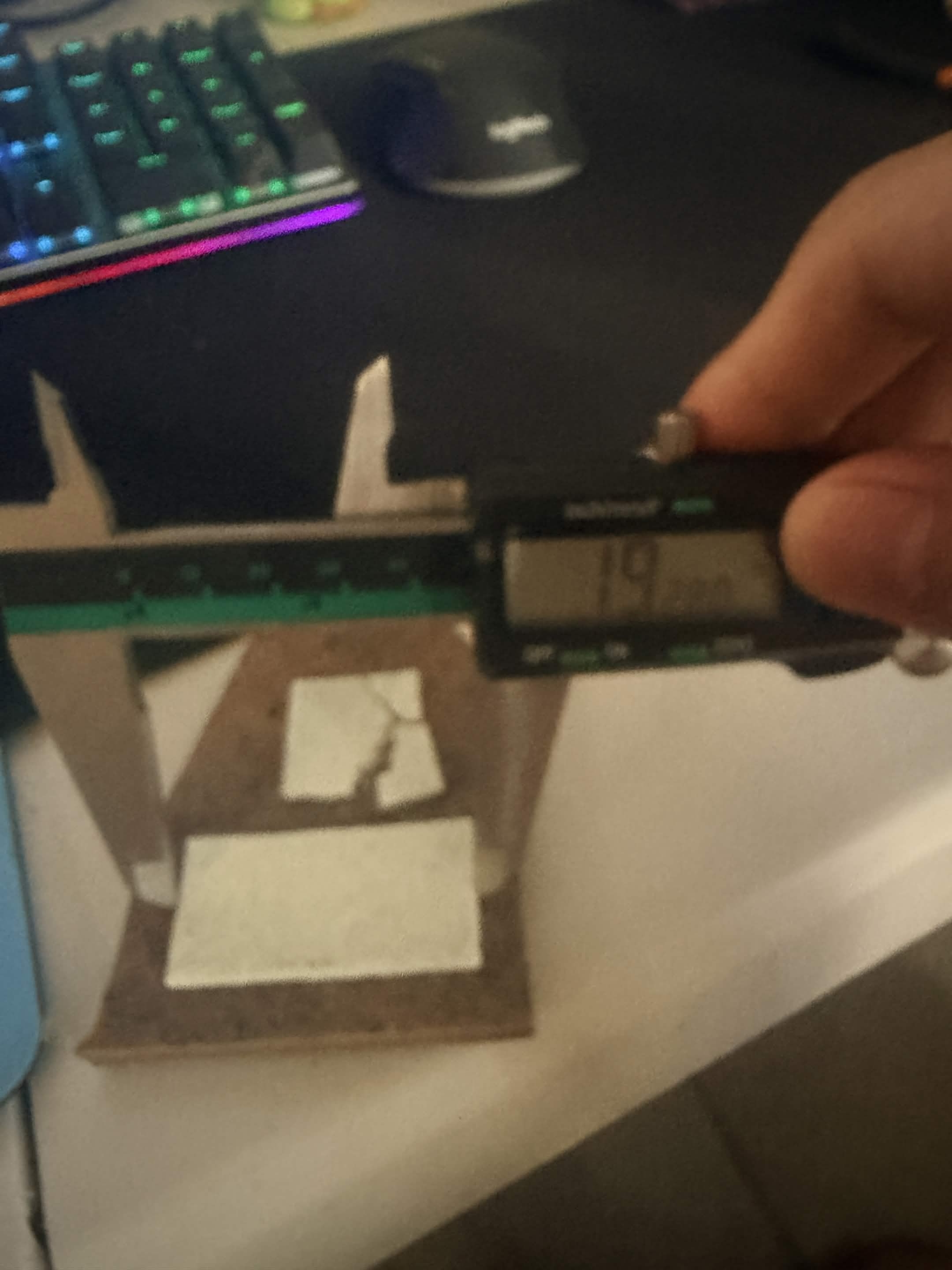
Fired glass: one number and one problem. Our latest borosilicate glass filament coupon showed approximately 10% linear shrinkage after firing.

That gives us an initial geometry-compensation factor, but it is not yet a complete process model. The next coupons will measure shrinkage independently in X, Y and Z and compare the final silver conductor dimensions with the surrounding glass.

Uniform and repeatable shrinkage is something we can compensate for mathematically. Differential shrinkage is the larger risk. If the glass and silver contract at different rates during the firing cycle, the result can be cracked parts, separated interfaces or open conductors. That mismatch has not yet been measured, and it is the next major experiment on the bench.

Using standardized IPC-7351 Nominal land patterns gives us a consistent starting geometry. We can then apply our own process compensation rather than redesigning every footprint independently.

The second result is less encouraging: the fired parts are extremely brittle. That does not automatically rule out the material, but it means durability has to become a measured engineering problem rather than something we assume will improve. We're separating the possible causes into firing schedule, residual porosity, part geometry, surface flaws and handling conditions, and we'll evaluate revised thermal cycles, annealing and surface sealing before committing to an additional production step.

Pressure-assisted firing will also remain an experimental variable rather than a fixed product requirement. Initial tests will stay coupon-scale because the required force rises rapidly with part area. We first need to determine whether pressure improves bonding without distorting printed traces or fracturing the glass.

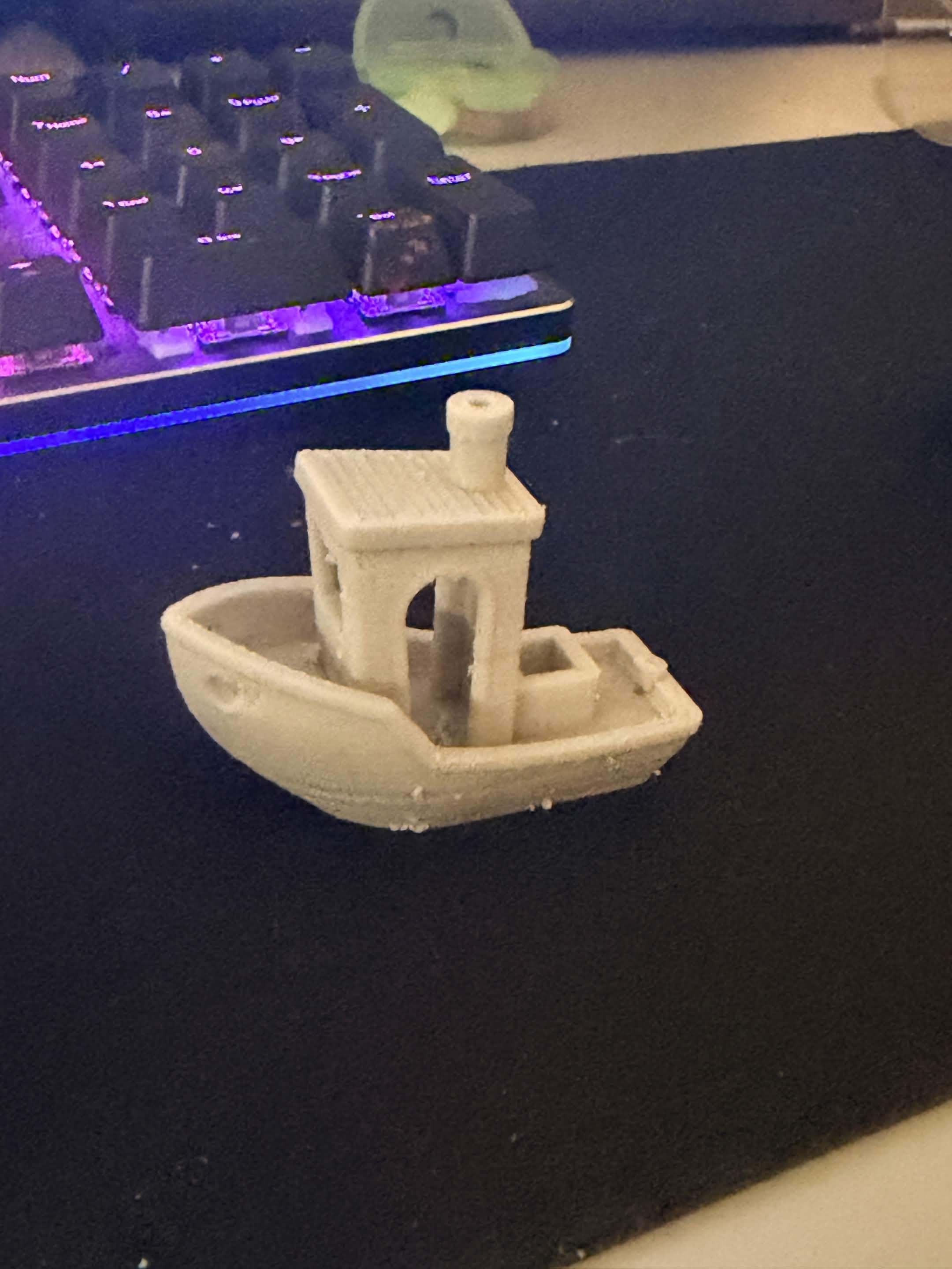
The next demonstration. The next functional test vehicle is still the glass Benchy, but the success criterion is not whether it looks like a boat. Silver conductors will be routed internally through the fired part and connected to pads on the exterior surface. We will then solder real SMT components to those pads. Success means:

  • The buried conductors retain continuity after firing.
  • The external pads remain solderable.
  • The part survives assembly without cracking.
  • The completed circuit operates.

At that point it stops being a demonstration of a printed shape with conductive material inside it. It becomes a circuit board that was never a board.

One known risk is solder leaching at exposed pure-silver pads. We therefore expect to use a leach-resistant Ag-Pd or Ag-Pt termination on external pads while retaining higher-conductivity silver in buried traces. Pad composition, solder alloy, temperature and dwell time will be tested as one system.

The motion problem is getting bounded and the material problem is getting measurable. The next milestone is making both meet in one functioning fired circuit.
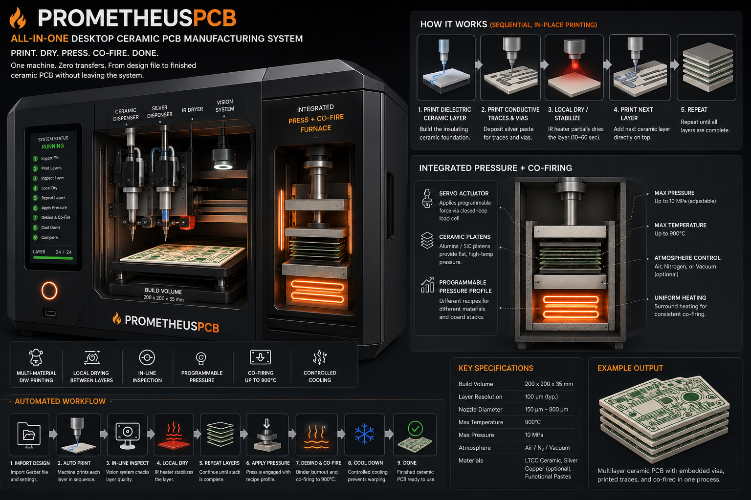
Concept poster for the PrometheusPCB all-in-one desktop ceramic PCB system, showing the machine, the print-dry-press-co-fire sequence, the integrated press and furnace, and key specifications.
Concept poster for the all-in-one system, refined with AI assistance: print, dry, press, co-fire, in one enclosure. This is a render of the machine we are building, not a photo of a finished one, and the specifications on it are targets rather than measured results. That includes the integrated press: pressure-assisted firing is still an experimental variable (see below), not a settled requirement.
Our assembled Open Micro-Manipulator on a desk: black printed frame, three stepper motors with white printed flexure arms, and a Raspberry Pi microcontroller board with stepper drivers.
Our build of the Open Micro-Manipulator, assembled and on the bench: parallel kinematics, NEMA-17 steppers, closed-loop controller, printed structural parts. Design by 0x23 (MIT); this unit is ours.
Animated CAD study of the micro-manipulator kinematics sweeping through its range of motion, showing the linkage rods, lever arms and ball-joint chains moving and where the mechanism runs into itself.
CAD motion study of the kinematics through its range. Where the linkages run into each other is what bounds the usable working volume, and that is what the motion architecture has to solve.
A 3DBenchy boat printed in borosilicate glass-filled filament, matte off-white, sitting on a desk mat.
3DBenchy printed in the borosilicate glass filament, the test article for the internally-routed silver build.
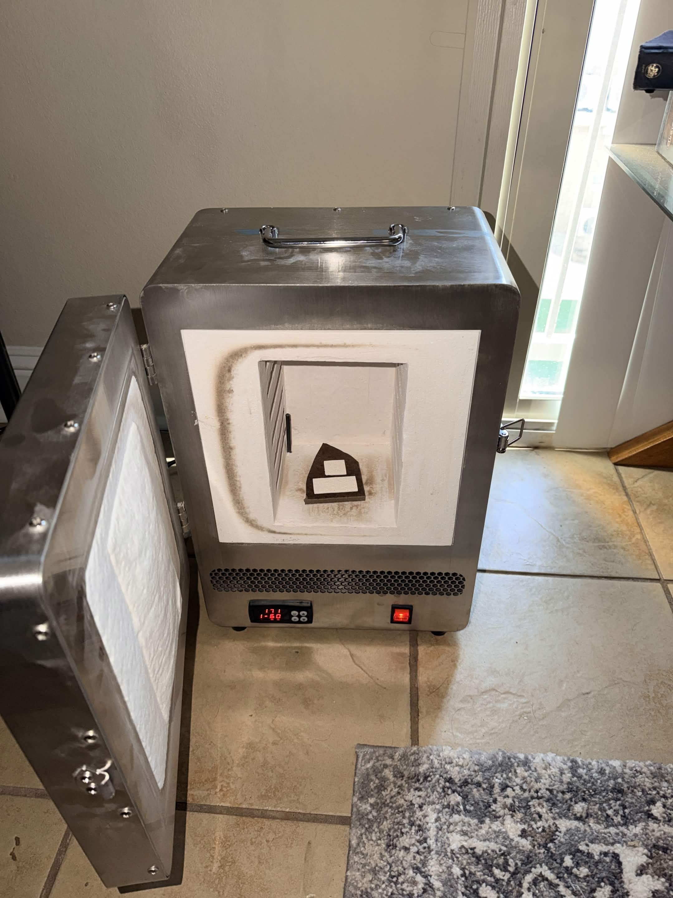
A small stainless bench kiln with its door open, showing a fired dark test article on white refractory board inside, controller reading temperature.
Bench kiln with a fired test article inside, the firing setup behind the shrinkage and brittleness results.
Digital calipers measuring a fired test article on a desk.
Post-fire dimensional check. Roughly 10% linear shrinkage in the fired glass, a provisional compensation factor, not yet a characterized one.
Open Micro-Manipulator on GitHub →

Next target: a functional 3DBenchy for YC

Research phase done. Now we build. The material and process questions we could settle on paper are settled; the next move is to make something real and put it in front of people.

Our first functional-object prototype is a 3D-printed 3DBenchy (the standard 3D-printing benchmark boat) with conductive traces and vias routed inside the model itself, and LEDs mounted on the outside surface, lit through the wiring buried in the print.

This first one is hand-built on purpose. Instead of waiting on a finished machine, we run the process ourselves, one step at a time: 3D-print the part, apply the conductor ink by hand into the channels, then co-fire it. Doing each step individually is how we prove the full sequence works end to end; folding those three steps into one automated pass is exactly what the machine is for.

To square this with the technical brief's paste-not-filament argument: printing the green body from glass-filled filament is a deliberate shortcut for these hand-run proofs, and a worst-case vehicle on purpose. The question on trial is whether an LTCC-style board can be made in-house at all, and filament is the least favorable green body we'll ever fire: more binder, less glass, more porosity than a formulated paste. If the circuit works in this body, a denser paste body should only improve it. Paste brings engineering of its own (rheology, layer flatness, fresh shrinkage numbers), but those are known problems with production precedent, not questions about whether the thing can exist. The conductor already goes down as dispensed ink, and the machine itself stays a direct-ink-writing design.

The point isn't the boat, it's the proof. Once the conductors live inside the printed geometry, the "circuit board" stops having to be a board at all: it can be any shape the part already is. The target is to finish by July 26 to anchor a Y Combinator application: a concrete milestone in hand, plus the bigger picture of where a machine that prints electronics inside the object can go.

Groundwork behind it. Repositioned the whole site around printed passives: the machine isn't just a PCB printer; it forms resistors, capacitors, and inductors directly in the ceramic layers, so the bulk of a board's BOM is fabbed, not placed. And for the parts we'll still place by hand, standardized on IPC-7351 footprints (Nominal (N) first, the industry default), to compensate later for our line width and shrinkage. First passive targets: 0402 / 0603 / 0805 R and C.

First silver ink ordered, and a coupon to measure it

First atoms in motion. Payment cleared and the Dycotec order is officially in: our first silver conductor ink, the metal that becomes the traces once it's printed and fired, is now in manufacture, with the ten-working-day clock from the Jul 10 signing running. Meanwhile we designed a dedicated trace-thickness test coupon to characterize it the day it arrives.

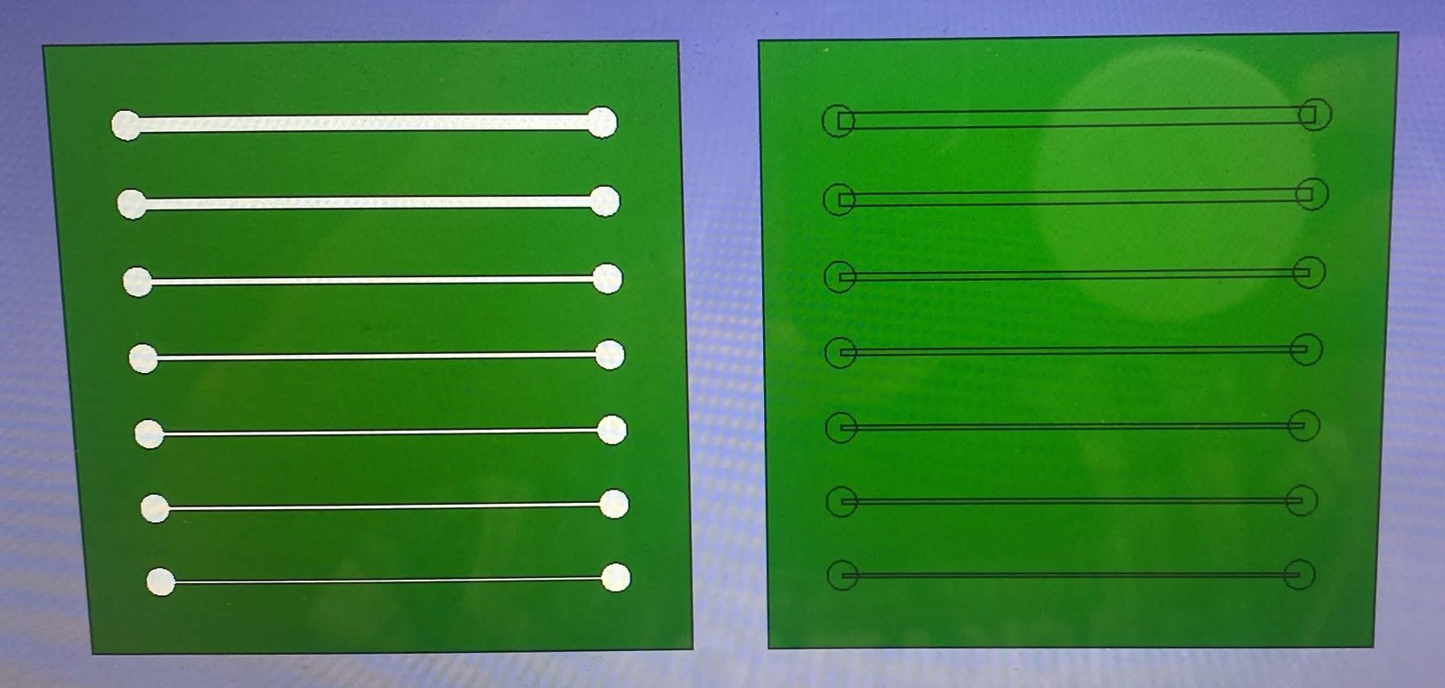
The coupon (pictured) is a set of straight traces stepped across a range of widths, each capped with probe pads at both ends. Print it, co-fire it, then measure: how much a fired trace shrinks from its drawn size, and what the final geometry does to conductivity and resistance.

That's the ground truth the rest of the process needs. Once we know the shrinkage factor and the sheet resistance of a real fired trace, we can compensate the drawn geometry to hit target dimensions and trust the electrical numbers, the same compensation the printed footprints and passives will lean on.

CAD view of the trace-thickness test coupon: two boards of straight traces stepped across a range of widths, each trace ending in circular probe pads.
TraceThickness test coupon (ProPCB): traces stepped across widths with probe pads at each end, for measuring fired shrinkage and trace resistance.

Signed with Dycotec for the silver: a custom fritless paste, and the education bundled in

The conductor has a supplier. After shopping thick-film paste makers for a silver that can co-fire in air around 850 °C on a borosilicate green body, we've signed with Dycotec Materials (UK). Nothing off the shelf fits, since standard silvers carry glass frit and are built for firing on pre-fired alumina, so the deal is a small custom batch made for us: DM-SIP-14001-K0, a fritless silver, plus a matched thinner for dispensing. The conductor side of the process is direct-ink-writing paste from day one, even while the green bodies for the hand-run proofs come off a filament printer.

Fritless is the decision worth logging. Conductor pastes normally carry frit to grip a substrate that's already dense and fired. Our case is inverted: the body is green glass that softens in the same firing, so the substrate itself provides the bond and added frit only complicates the interface chemistry. Dycotec's engineers landed on the same call before we'd shared our instinct, which is the agreement you want to see before spending materials budget.

The order is as much tuition as material. Part of the point is a deliberate investment in the materials science of how a conductor behaves in this machine, and the spec exchange alone retired real unknowns: fineness of grind under 10 µm (comfortable through our 300–400 µm nozzles), a 400–450 °C binder-burnout window that now anchors the front of our firing profile ahead of the 850 °C peak, thinner on hand because screen-printing rheology isn't dispensing rheology, and pure silver for now; leach-resistant Ag-Pd terminations can wait until solderability is the question on the bench. Each answer is a coupon we don't have to ruin to learn the same thing.

The honest terms: it's a best-efforts batch. Dycotec hasn't fired on a green borosilicate body any more than we have, and there's no technical datasheet until the material exists. About $850 all-in of JumpStart money for 75 g of paste, thinner, and shipping, on roughly a ten-working-day manufacture. We're buying an experiment, not a guaranteed component, and we'd make that trade again.

Dycotec Materials →

Julian Stoller joined as co-founder

Picked up a co-founder: Julian Stoller, a fresh Cornell mechanical-engineering graduate with deep additive-manufacturing experience (the deposition and process side of building a machine like this), which pairs directly with the electrical-systems side of the work. The match came through Y Combinator's Co-Founder Matching, and we'd been building together for weeks before making it official. From here we're tackling PrometheusPCB together.

Julian on LinkedIn →

Post-fire metallization as the documented fallback

Committed to carrying a backstop for the co-fire shrinkage-mismatch risk: print and fire the ceramic first, then metallize afterward. Costs some density and layer count, but it sidesteps the mismatch entirely, so the program isn't betting everything on cracking constrained sintering on day one.

LTCC over HTCC: staying under 900 °C

Chose low-temperature co-fired ceramic (850–900 °C) over HTCC (1400–1600 °C). The LTCC window sits just below silver's melting point, which is what lets us co-fire silver, copper, and gold, the low-resistivity conductors you actually want for RF and high-speed digital. HTCC would force refractory metals at ~10× the resistivity. Everything downstream follows from staying in that window.

The reasoning, in the technical brief →

Backed by TTU JumpStart + NSF I-Corps

PrometheusPCB picked up Texas Tech Innovation Hub JumpStart funding and an NSF I-Corps customer-discovery grant, enough room to start chasing the gap now instead of someday. Kicked off customer discovery with hardware teams and labs.

Project kickoff

Started PrometheusPCB. The thesis: pull ceramic fabrication onto the bench so the wait between revisions stops being the bottleneck. Solo for now, and already looking for a materials co-founder who reads the shrinkage problem as a challenge rather than a dealbreaker.